
This content originally appeared on DEV Community and was authored by LambdaMamba
Hello everyone!
In the last post, Getting started with FPGA projects on Intel® Quartus Prime, I went through the basics of creating FPGA projects and digital circuits. However, the lack of inputs and outputs on the FPGA really limits the digital circuit's complexity and creativity.
To overcome this constraint, I decided to use the external GPIO pins on my DE10 Nano FPGA. Thus in this tutorial, I will be going through the steps required to use external inputs and outputs for the FPGA. If at any stage you get lost with the Quartus operations during this tutorial, visit my previous post for details on how to use Quartus.
Table Of Contents
- Finite State Machine with external inputs and outputs
- Morse Code Translator with external inputs and outputs
Finite State Machine with external inputs and outputs
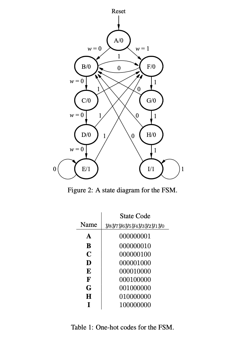
I will be using the Intel Laboratory Exercise 7, Finite State Machines. Here, we would like to implement Part I of Intel's Exercise 7, where the FSM looks like the following.
Assuming that you have familiarised yourself with Verilog HDL, the Verilog HDL code I wrote for this exercise would be in my Github.
Before uploading the digital circuit to the FPGA, we would like to test if the state transitions and signals show up as expected.
We will be using a simulator called ModelSim, and will require the use of a test bench file. This part is optional and can be skipped, however, it is really difficult to pinpoint errors in the logic without ModelSim, so I recommend using it for complex logic circuits.
This test bench part was tricky when I started the FPGA projects, so I highly recommend watching Intel's Tutorial on generating a test bench on ModelSim to become familiar with ModelSim and test benches.
I wrote the test bench file in Verilog HDL, and is shown here in my Github. If everything goes as expected, the signals should look something like this.

Now comes the fun part, uploading the digital circuit onto the FPGA. I used the following inputs and outputs for this project,
- DE10 Nano User button for the clock
- External Slide Switch for reset
- External Slide Switch for input w Outputs:
- External LED0-LED8 for showing state code
- External LED9 for output z
For 2-3, I got a SS12D00G5 slide switch. For 4, I got a 3mm 20 mA White LED. For 5, I got a 3mm 20 mA red LED. You don't have to worry too much about the LED's voltage as long as it is within the 2-3 V range. A higher voltage may result in dimmer light, but should still be visible. I also got myself a breadboard, male-female jumper wires, and a few small resistors (not really necessary, just there to control the brightness of the LED). For the reset, I have decided to use an active low synchronous reset (which means simply sliding the switch does not reset it, but will reset when I press the clock button).
Use the male-female connectors to wire the GPIO pins to the breadboard. The GPIO pin names should be available in your FPGA's manual, and try to keep track of them while you are wiring your breadboard. I am using the DE10 Nano, and my circuit ended up looking like this.

Also, make sure to connect the ground to the GND GPIO. After finishing the circuit construction, double click on Analysis & Synthesis. Upon completion, go to the Pin Planner, and assign the pins accordingly.

Compile the Design, and once everything succeeds, go to the Programmer and press Start. If successful, the circuit should behave somewhat similar to the demo shown below.

In the demo, the state transition is A > B > C > D > E > reset > A > F > G > H > I. The red LED z lights up if 0 or 1 is inputted from the slide switch 4 or more times consecutively, thus the red LED lights up on state E and I. For the clock, I am manually pressing the user button on the DE10 nano. Also, ignore the 8 slide switches on the left because they are not used in this project.
Morse Code Translator with external inputs and outputs
I will go through another FPGA project I worked on a few years ago while ago, which is the Morse Code Translator. I implemented a subset of morse codes as shown below.

And I came up with the following state transition diagram.

For this project, I used a 7 segment display. As I could not find the specifications for this component, I manually tested the 7 segment display to find out which signals give which letters/numbers.

To make the morse code translator as realistic as possible, I decided to distinguish between the dot and dash depending on how long the button is pressed. A button that is pressed and released instantaneously would be registered as a dot, while a button that is pressed and held on for more than a second will be registered as a dash. To implement a time-dependent digital circuit, I made use of a Clock Divider, which divides the FPGA's Clock (50 MHz for a DE10 Nano) to count time in the millisecond range. You can see my Morse Verilog Code on Github for more details.
For the circuit, I used two segment displays, one to show whether the button press registered as a dot or dash, and another to display the translated character or an intermediate state. The circuit diagram I used looks like the following.

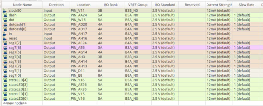
In addition to the external inputs and outputs, I used the DE10 Nano's Clock, LEDs and Buttons, so the pin planner should look something like the following.
In this first demo, the state transitions {s0 > E > s5 > s7 > H >(reset) s0} takes place.

E: .
s5: ..
s7: ...
H: .
In this second demo, the state transitions {s0 > E > s5 > s6 > F} takes place.

E: .
s5: ..
s6: ..-
F: ..-.
In this third demo, the state transitions {s0 > s1 > s3 > s4 > C} takes place.

s1: -
s3: -.
s4: -.-
C: -.-.
What's next?
Being able to use external inputs and outputs allows for fancy FPGA projects, and also helps with debugging. Back in 2020, I wrote a MIPS 5-Stage Pipeline CPU that accepts user inputs in Verilog HDL, and ran a Fibonacci Program. The use of external inputs and outputs made the debugging process much easier, as I was able to see what was going on inside the CPU, as well as its memory and register contents.

I may write a tutorial on creating a CPU in Verilog HDL that accepts user inputs, and in the meanwhile, I highly suggest reading through Digital Design and Computer Architecture by David Harris & Sarah Harris as it explains the construction of a CPU in Verilog HDL.
Thank you for reading! Good luck with your FPGA projects, and have fun creating your circuits!
I would love to see your creations on the FPGAs, so please feel free to post them here!
This content originally appeared on DEV Community and was authored by LambdaMamba
LambdaMamba | Sciencx (2021-08-14T18:47:19+00:00) Making fancy FPGA projects with external I/O using the GPIO. Retrieved from https://www.scien.cx/2021/08/14/making-fancy-fpga-projects-with-external-i-o-using-the-gpio/
Please log in to upload a file.
There are no updates yet.
Click the Upload button above to add an update.